

Park Systems is a world-leading manufacturer of nanometrology tools for surface analysis in research and industry.
Joined November 2011
- Tweets4.3K
- Following1.1K
- Followers7.9K
- Likes368


[𝗡𝗮𝗻𝗼𝘀𝗰𝗮𝗹𝗲 𝗘𝗹𝗲𝗰𝘁𝗿𝗼𝗰𝗵𝗲𝗺𝗶𝘀𝘁𝗿𝘆: 𝗦𝗘𝗖𝗖𝗠 𝗪𝗲𝗲𝗸 / 𝗘𝗽𝗶𝘀𝗼𝗱𝗲 𝟱]
SECCM can go beyond arrays of point measurements to map surface topography and electrochemical activity simultaneously.
In this application note, researchers from Texas A&M University and Park Systems demonstrate a 𝗱𝗼𝘂𝗯𝗹𝗲-𝗯𝗮𝗿𝗿𝗲𝗹𝗹𝗲𝗱 𝗽𝗶𝗽𝗲𝘁𝘁𝗲 𝘀𝗲𝘁𝘂𝗽, with a separate quasi-reference counter electrode in each channel.
This configuration helps maintain consistent meniscus geometry during scanning, enabling simultaneous mapping of topography and local electrochemical response.
💡𝗘𝘅𝗽𝗹𝗼𝗿𝗲 𝘁𝗵𝗲 𝘀𝗲𝘁𝘂𝗽 𝗶𝗻 𝘁𝗵𝗲 𝗳𝘂𝗹𝗹 𝗮𝗽𝗽𝗹𝗶𝗰𝗮𝘁𝗶𝗼𝗻 𝗻𝗼𝘁𝗲: okt.to/nNxbkd
#ElectrochemistryWeeks #SECCM #Electrochemistry #Nanoelectrochemistry #ScanningProbeMicroscopy

124
[𝗡𝗮𝗻𝗼𝘀𝗰𝗮𝗹𝗲 𝗘𝗹𝗲𝗰𝘁𝗿𝗼𝗰𝗵𝗲𝗺𝗶𝘀𝘁𝗿𝘆: 𝗦𝗘𝗖𝗖𝗠 𝗪𝗲𝗲𝗸 / 𝗘𝗽𝗶𝘀𝗼𝗱𝗲 𝟰]
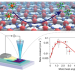
AFM is an ideal technique to study the morphology and functional properties of heterostrucutres of layered materials, with SECCM extending even to their electrochemical properties!
In this 𝗡𝗮𝘁𝘂𝗿𝗲 𝗖𝗵𝗲𝗺𝗶𝘀𝘁𝗿𝘆 𝗽𝗮𝗽𝗲𝗿, researchers from the University of California, Berkeley, Brown University, and Carnegie Mellon University combined scanning tunnelling microscopy (STM) measurements of twist angle with SECCM measurements on a Park NX10 to explore twisted bilayer graphene supported on hexagonal boron nitride.
Their findings show that changing the angle between the graphene layers tunes their electrochemical response, demonstrating how “twistronics” can modify surface reactivity.
📜𝗥𝗲𝗮𝗱 𝘁𝗵𝗲 𝗽𝗮𝗽𝗲𝗿 𝗵𝗲𝗿𝗲: okt.to/QuDbLt
#ElectrochemistryWeeks #SECCM #Electrochemistry #Twistronics #Graphene #2DMaterials

[𝗡𝗮𝗻𝗼𝘀𝗰𝗮𝗹𝗲 𝗘𝗹𝗲𝗰𝘁𝗿𝗼𝗰𝗵𝗲𝗺𝗶𝘀𝘁𝗿𝘆: 𝗦𝗘𝗖𝗖𝗠 𝗪𝗲𝗲𝗸 / 𝗘𝗽𝗶𝘀𝗼𝗱𝗲 𝟯]
What can a single material flake reveal that an aggregate might hide?
A 𝗸𝗲𝘆 𝗮𝗱𝘃𝗮𝗻𝘁𝗮𝗴𝗲 𝗼𝗳 𝗦𝗘𝗖𝗖𝗠 over macroscopic measurements is its ability to probe small, localized regions. This allows researchers to explore the contributions of features such as defects and step edges, and to study individual 2D material flakes separately from their aggregates.
In a study published in 𝗡𝗮𝘁𝘂𝗿𝗲 𝗖𝗼𝗺𝗺𝘂𝗻𝗶𝗰𝗮𝘁𝗶𝗼𝗻𝘀, researchers from Trinity College Dublin and Victoria University of Wellington used SECCM on a Park NX10 to investigate monolayer MXene flakes. Their findings suggest rapid proton transport across the flake surface, providing insights relevant to the use of MXenes in energy storage devices.
📜𝗥𝗲𝗮𝗱 𝘁𝗵𝗲 𝗳𝘂𝗹𝗹 𝗽𝗮𝗽𝗲𝗿: okt.to/raWTeo
#ElectrochemistryWeeks #SECCM #Electrochemistry #MXenes #2DMaterials #EnergyStorage

1
172
[𝗡𝗮𝗻𝗼𝘀𝗰𝗮𝗹𝗲 𝗘𝗹𝗲𝗰𝘁𝗿𝗼𝗰𝗵𝗲𝗺𝗶𝘀𝘁𝗿𝘆: 𝗦𝗘𝗖𝗖𝗠 𝗪𝗲𝗲𝗸 / 𝗘𝗽𝗶𝘀𝗼𝗱𝗲 𝟮]
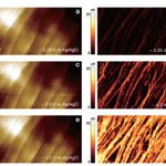
SECCM’s nanoscale resolution and ability to address specific features on a surface open up new possibilities for exploring fundamental electrochemical processes.
In this 𝗡𝗮𝘁𝘂𝗿𝗲 𝗽𝗮𝗽𝗲𝗿, researchers at the University of California, Berkeley, used SECCM on a Park NX10 to investigate how doping changes the electrochemical response of graphene.
Their findings reveal that the electrode’s electronic density of states plays a more significant role in governing interfacial electron-transfer reactivity than previously understood.
📜Read the full paper: okt.to/mzh7Xr
#ElectrochemistryWeeks #SECCM #Electrochemistry #Graphene #ElectronTransfer #Nanoelectrochemistry

1
105
[𝗡𝗮𝗻𝗼𝘀𝗰𝗮𝗹𝗲 𝗘𝗹𝗲𝗰𝘁𝗿𝗼𝗰𝗵𝗲𝗺𝗶𝘀𝘁𝗿𝘆: 𝗦𝗘𝗖𝗖𝗠 𝗪𝗲𝗲𝗸 / 𝗘𝗽𝗶𝘀𝗼𝗱𝗲 𝟭]
What could mapping electrochemical responses at the nanoscale reveal about your samples? This week, we’re exploring scanning electrochemical cell microscopy (SECCM) and how local measurements can help distinguish the effects of sample heterogeneity from fundamental limits on material performance limitations.
Park’s NX series AFMs can be equipped with a dedicated head for SECCM and other pipette-based modes, bringing nanoscale electrochemical measurements to your research.
💡𝗖𝘂𝗿𝗶𝗼𝘂𝘀 𝗮𝗯𝗼𝘂𝘁 𝗵𝗼𝘄 𝗶𝘁 𝘄𝗼𝗿𝗸𝘀? 𝗦𝘁𝗮𝗿𝘁 𝘄𝗶𝘁𝗵 𝗼𝘂𝗿 𝗮𝗽𝗽𝗹𝗶𝗰𝗮𝘁𝗶𝗼𝗻 𝗻𝗼𝘁𝗲: okt.to/VlSNTA
📜Ready to explore the practical side? 𝗧𝗵𝗶𝘀 𝗔𝗖𝗦 𝗠𝗲𝗮𝘀𝘂𝗿𝗲𝗺𝗲𝗻𝘁 𝗦𝗰𝗶𝗲𝗻𝗰𝗲 𝗔𝘂 𝘁𝘂𝘁𝗼𝗿𝗶𝗮𝗹 featuring Park’s NX12 provides a comprehensive introduction to hands-on SECCM protocols: okt.to/Wtv5og
#ElectrochemistryWeeks #SECCM #Electrochemistry #Nanoelectrochemistry #ScanningProbeMicroscopy

[📢 𝗙𝗶𝗻𝗮𝗹 𝗖𝗮𝗹𝗹] Discover how 𝗗𝗶𝗴𝗶𝘁𝗮𝗹 𝗛𝗼𝗹𝗼𝗴𝗿𝗮𝗽𝗵𝗶𝗰 𝗠𝗶𝗰𝗿𝗼𝘀𝗰𝗼𝗽𝘆 (𝗗𝗛𝗠) goes beyond conventional 2D imaging to capture dynamic three-dimensional processes without mechanical Z-scanning.
Join our webinar to explore high-speed, label-free volumetric imaging from a single hologram, enabling quantitative analysis of 3D cell and microorganism tracking, particle tracking for flow characterization, and depth-resolved inspection of transparent materials.
📅 November 17, 2026
🔗 𝗥𝗲𝗴𝗶𝘀𝘁𝗲𝗿 𝗡𝗼𝘄: okt.to/ZOGnAt
#DHM #DigitalHolographicMicroscopy #3DImaging #4DImaging #LifeScience #FluidDynamics #MaterialsScience #ParkSystems

Why automation in research AFM?
Imagine navigating between loaded samples without adjusting knobs or manually locating each measurement site. Park FX AFMs make it possible.
Watch how a calibrated alignment camera above the motorized sample stage maps samples on the chuck and defines locations for automated measurements.
💡Map all samples loaded on the instrument
💡Mark stage coordinates for later automated measurements
💡Switch between samples remotely
These features support multi-sample workflows and navigation on large substrates, including 200 mm wafers.
𝗘𝘅𝗽𝗹𝗼𝗿𝗲 𝗺𝗼𝗿𝗲 𝗙𝗫 𝗮𝘂𝘁𝗼𝗺𝗮𝘁𝗶𝗼𝗻 𝗳𝗲𝗮𝘁𝘂𝗿𝗲𝘀 𝗮𝗻𝗱 𝗱𝗲𝗺𝗼 𝘃𝗶𝗱𝗲𝗼𝘀: okt.to/7qAos2
193
How much 3D motion is lost in a 2D image?
Join our November 17 webinar to explore how DHM enables 4D tracking of cells, microorganisms, and particles, plus depth-resolved 3D inspection of transparent materials.
🔗 Register now: okt.to/oeT7Un
#DHM #4DTracking #LifeScience #FluidDynamics #MaterialsScience

Small deformations, valuable electrochemical insights.
Learn how Electrochemical Strain Microscopy (ESM) detects local swelling due to the flow of ionic and electronic changes in conducting polymers and battery materials.
👉𝗦𝗮𝘃𝗲 𝘆𝗼𝘂𝗿 𝘀𝗲𝗮𝘁: okt.to/qy7js1
#ElectrochemicalStrainMicroscopy #AFM #Electrochemistry #BatteryResearch

Day 2 at 𝗦𝗘𝗠𝗜𝗖𝗢𝗡 𝗘𝘂𝗿𝗼𝗽𝗮, and we’re ready to talk metrology!
Visit Park Systems at Booth C1-501 to meet our team and discuss solutions for your semiconductor applications:
• 𝗡𝗫-𝗪𝗮𝗳𝗲𝗿: automated in-line AFM for wafer surface metrology
• 𝗡𝗫-𝗠𝗮𝘀𝗸: AFM-based photomask defect repair
• 𝗡𝗫-𝗧𝗦𝗛: automated AFM for panel-level packaging, handling panels up to 600 × 600 mm
• 𝗡𝗫-𝗛𝘆𝗯𝗿𝗶𝗱 𝗪𝗟𝗜: integrated AFM and white light interferometry, combining large-area optical profiling with precise nanoscale measurements
• 𝗔𝗰𝗰𝘂𝗿𝗶𝗼𝗻 𝗘𝗣𝟰: imaging spectroscopic ellipsometry for mapping thin-film thickness and refractive index
From wafer processing to advanced packaging, let’s discuss your samples, measurement requirements and automation needs.
Stop by, say hello and tell us what you’re working on!
📍 Messe München | Booth C1-501
#SEMICONEuropa #ParkSystems #Semiconductor #Metrology


1
288
Why choose an automated AFM?
Save time on probe loading, exchange and alignment with Park Systems’ FX series AFMs.
Watch the video to see probe loading, QR code recognition, pickup, detection and alignment, all fully automated.
💡Switch between preloaded probes remotely during long automated experiments
💡Automatically identify probe types using QR codes
💡Focus on exploring the technique with less time spent on setup
💡Reduce the risk of user error during probe handling and alignment
𝗘𝘅𝗽𝗹𝗼𝗿𝗲 𝗺𝗼𝗿𝗲 𝗙𝗫 𝗮𝘂𝘁𝗼𝗺𝗮𝘁𝗶𝗼𝗻 𝗳𝗲𝗮𝘁𝘂𝗿𝗲𝘀 𝗮𝗻𝗱 𝗱𝗲𝗺𝗼 𝘃𝗶𝗱𝗲𝗼𝘀: okt.to/fy2owr
105
Join our upcoming webinar to discover how 𝗗𝗶𝗴𝗶𝘁𝗮𝗹 𝗛𝗼𝗹𝗼𝗴𝗿𝗮𝗽𝗵𝗶𝗰 𝗠𝗶𝗰𝗿𝗼𝘀𝗰𝗼𝗽𝘆 (𝗗𝗛𝗠) enables fast, label-free, and quantitative 3D volumetric imaging and 4D time-resolved tracking.
Learn how DHM captures three-dimensional information from a single hologram without mechanical Z-scanning, enabling high-speed analysis of dynamic processes in biological and material systems, including cell tracking, flow characterization, and transparent material inspection.
📅 November 17, 2026
🔗 𝗥𝗲𝗴𝗶𝘀𝘁𝗲𝗿 𝗻𝗼𝘄: okt.to/IXnYzG
#DHM #DigitalHolographicMicroscopy #3DImaging #4DImaging #LifeScience #FluidDynamics #MaterialsScience #ParkSystems

New office, new momentum for 𝗣𝗮𝗿𝗸 𝗦𝘆𝘀𝘁𝗲𝗺𝘀 𝗝𝗮𝗽𝗮𝗻!
On October 30, 𝘄𝗲 𝗰𝗲𝗹𝗲𝗯𝗿𝗮𝘁𝗲𝗱 𝘁𝗵𝗲 𝗼𝗽𝗲𝗻𝗶𝗻𝗴 𝗼𝗳 𝗼𝘂𝗿 𝗿𝗲𝗹𝗼𝗰𝗮𝘁𝗲𝗱 𝗧𝗼𝗸𝘆𝗼 𝗼𝗳𝗳𝗶𝗰𝗲 with colleagues, partners and guests from universities and research institutions. This milestone strengthens our presence in Japan and celebrates the relationships that drive scientific progress.
And what better way to welcome this next chapter than with a Japanese tradition of 𝗞𝗮𝗴𝗮𝗺𝗶 𝗕𝗶𝗿𝗮𝗸𝗶? With wooden mallets in hand, we opened the lid of a sake barrel in a ceremony symbolizing good fortune, prosperity and new beginnings. A joyful way to celebrate our shared success!
Thank you to everyone who joined us. Here’s to stronger partnerships, shared discoveries and continued growth together! 🎉
#ParkSystems #ParkSystemsJapan #NewBeginnings


1
1,329
Our 𝗦𝗽𝗼𝘁𝗹𝗶𝗴𝗵𝘁 𝗰𝗮𝗺𝗲𝗿𝗮 is back in the USA, this time in sunny California! Meet 𝗘𝗱𝗱𝘆 𝗥𝗼𝗯𝗶𝗻𝘀𝗼𝗻, Director of Business Development for Optical Metrology and Spectroscopy.
Since joining Park Systems in January 2026, Eddy has enjoyed exploring how Park’s novel technologies can drive development and improve production efficiency. Just as rewarding is working again with an experienced team of AFM and metrology experts, some with roots in the early days of scanning probe microscopy.
And Eddy feels right at home in California! “I am a technology geek, so I’m perfectly suited to the San Francisco Bay Area.”
Outside of work, he loves exploring California’s great outdoors with his family, from Monterey Bay to the Sierra Nevada.
𝗧𝗵𝗮𝗻𝗸 𝘆𝗼𝘂, 𝗘𝗱𝗱𝘆, 𝗳𝗼𝗿 𝗯𝗿𝗶𝗻𝗴𝗶𝗻𝗴 𝘆𝗼𝘂𝗿 𝗽𝗮𝘀𝘀𝗶𝗼𝗻, 𝗳𝗿𝗲𝘀𝗵 𝗽𝗲𝗿𝘀𝗽𝗲𝗰𝘁𝗶𝘃𝗲𝘀, 𝗮𝗻𝗱 𝗲𝗻𝘁𝗵𝘂𝘀𝗶𝗮𝘀𝗺 𝘁𝗼 𝘁𝗵𝗲 𝗣𝗮𝗿𝗸 𝗳𝗮𝗺𝗶𝗹𝘆! ♥️
#TeamSpotlight #PeopleBehindTheBrand #MeetTheTeam #ParkSystems #ParkSystemsAmericas #OpticalMetrology #Spectroscopy #LifeAtPark
156
How do ions and electrons move through materials that conduct both?
Mixed ionic-electronic conductors play a key role in energy storage, bioelectronics and neuromorphic computing. Understanding how charge carriers move through these materials at the nanoscale is essential for their development.
Join 𝗣𝗿𝗼𝗳. 𝗧𝗼𝗯𝗶𝗮𝘀 𝗖𝗿𝗮𝗺𝗲𝗿 (𝗨𝗻𝗶𝘃𝗲𝗿𝘀𝗶𝘁𝘆 𝗼𝗳 𝗕𝗼𝗹𝗼𝗴𝗻𝗮) to explore how advanced AFM techniques reveal ionic and electronic transport processes in-operando.
Discover what nanoscale strain measurements can tell us about mixed ionic-electronic conductors.
👉Register now: okt.to/FDI054
#Electrochemistry #AFM #MaterialsScience #EnergyStorage

121
An AFM image is not yet a measurement. Learn how to move from imaging to data interpretation in our 𝟰𝟱-𝗺𝗶𝗻𝘂𝘁𝗲 𝘄𝗼𝗿𝗸𝘀𝗵𝗼𝗽 at the XV International NanoAndes School in Bariloche.
📅Friday, 6 November 2026 · 14:00 (Argentina time, UTC−3)
📍Instituto Balseiro, Centro Atómico Bariloche
𝗕𝗿𝗶𝗻𝗴 𝘆𝗼𝘂𝗿 𝗱𝗮𝘁𝗮!
The session ends with a Data Clinic. Bring an AFM image or dataset that is hard to interpret, on a USB drive or as a link. We will review artifacts, processing choices and interpretation together.
👉 𝗕𝗼𝗼𝗸 𝗮 𝘀𝗹𝗼𝘁: okt.to/nOWjTB
#NanoAndes2026 #AFM #2DMaterials #Nanotechnology #ParkSystems

2
2,562
Fine-pitch hybrid bonding is making surface preparation critical: manufacturers must control copper pad recess and dielectric smoothness at the nanometre scale to achieve reliable 3D chip integration.
Meet our European industrial sales team at 𝗦𝗘𝗠𝗜𝗖𝗢𝗡 𝗘𝘂𝗿𝗼𝗽𝗮 𝟮𝟬𝟮𝟲 in Munich to explore automated atomic force microscopy for semiconductor manufacturing—from wafer surface characterization to process monitoring and failure analysis.
Bring your application questions and discuss measurement requirements, automation, and fab integration with @Lars Vitense, @Romain Bourrellier and @Ludger Weisser.
📍 Messe München | Booth C1-501
📅 10–13 November 2026
Planning your visit? Send us a message to arrange a meeting, or stop by our booth.
💡𝗘𝘅𝗽𝗹𝗼𝗿𝗲 𝘄𝗵𝗮𝘁 𝘄𝗲’𝗹𝗹 𝗯𝗲 𝗽𝗿𝗲𝘀𝗲𝗻𝘁𝗶𝗻𝗴:
okt.to/5Sbs8z
We look forward to seeing you in Munich!
#SEMICONEuropa #ParkSystems #semiconductor #AFM #Metrology

[📢𝗙𝗶𝗻𝗮𝗹 𝗰𝗮𝗹𝗹] Join us for a closer look at battery interfaces and interphases at the nanoscale.
Our guest speaker, Prof. Dr. @Christine Kranz, Ulm University, will show how SECCM, conductive AFM, electrochemical AFM and nanomechanical mapping can reveal SEI formation, local mechanical properties and real-time structural changes in battery electrodes.
👉Secure your spot: okt.to/8RUO0x
#Electrochemistry #BatteryResearch #SECCM #AFM #EnergyStorage

150
Thank you to QAV Technologies for hosting our 𝗔𝗙𝗠 𝘄𝗼𝗿𝗸𝘀𝗵𝗼𝗽 in Penang, Malaysia, at the end of October, and to all participants for bringing your samples, questions, and expertise!
Live demo sessions brought AFM into practice, exploring surface roughness and film thickness on participants’ own samples. Participants discussed applications, with strong interest in 𝗻𝗮𝗻𝗼𝗜𝗥 𝗳𝗼𝗿 𝗻𝗮𝗻𝗼𝘀𝗰𝗮𝗹𝗲 𝗰𝗵𝗲𝗺𝗶𝗰𝗮𝗹 𝗮𝗻𝗮𝗹𝘆𝘀𝗶𝘀 and 𝗠𝗮𝗴𝗻𝗲𝘁𝗶𝗰 𝗙𝗼𝗿𝗰𝗲 𝗠𝗶𝗰𝗿𝗼𝘀𝗰𝗼𝗽𝘆 (𝗠𝗙𝗠) for 𝗵𝗮𝗿𝗱 𝗱𝗶𝘀𝗸 𝗺𝗲𝗱𝗶𝗮 𝗰𝗵𝗮𝗿𝗮𝗰𝘁𝗲𝗿𝗶𝘇𝗮𝘁𝗶𝗼𝗻.
Great to see interest across Malaysia in advanced technologies for semiconductor failure analysis and materials characterization.
#AFM #nanoIR #MFM #Semiconductor #ParkSystems


1
1,956
🎃 Happy Halloween from Park Systems!
This year, we’re decorating at the nanoscale! These pumpkins were patterned on silicon using grayscale local anodic oxidation with our SmartLitho lithography package. By setting different patterning conditions at different locations, SmartLitho enables controlled variations in oxide thickness, bringing Halloween designs to life at the nanoscale.
𝗗𝗶𝘀𝗰𝗼𝘃𝗲𝗿 𝘄𝗵𝗮𝘁’𝘀 𝗽𝗼𝘀𝘀𝗶𝗯𝗹𝗲 𝘄𝗶𝘁𝗵 𝗦𝗺𝗮𝗿𝘁𝗟𝗶𝘁𝗵𝗼: okt.to/3PAoCE
#HappyHalloween #SmartLitho #Nanolithography #AFM #Nanotechnology #ParkSystems
