






Lip-Bu Tan on Intel Server CPUs:
Diamond Rapids is 2027.
Coral Rapids is 2028.
(During Earnings Call, Q3 2026.)
More on X86S Unified Core:
This is exciting! Top CPU architect Peter Bannon (who worked with Jim Keller on Apple Silicon A4 & A5) is the one working on the new X86S Unified Core in Rosaic in collaboration with Intel.
The plan is to develop the new high-performance core in a fast & independent manner (like startup mode without any hindrance) and later spin the team right back into Intel with the upgraded core IP.
A genius move by Lip-Bu!!!
Our big man is making so many amazing moves, it's just wild. A move that can give Intel a solid edge over competition.
Image Credit: VideoCardz

My predictions:
Zen 6 -> 6.0 to 6.2 GHz
Nova Lake -> 6.0 to 6.2 GHz
Zen 6 refresh -> Up to 6.8 GHz
Razor Lake -> Up to 6.5 GHz
I’ve seen people constantly underestimate TSMC N2X. N2X is set to have the highest Fmax (better than Intel 7), which directly benefits Zen 6 refresh (and not NVL).
Do not underestimate N2X when TSMC openly claims +10% higher Fmax!!!
More 👇

AMD Zen 6 (r) actually targets 7.0 GHz
First off, both Intel Nova Lake & AMD Zen 6 are both on TSMC N2P. So, both of them are expected to top out at 6.0 - 6.2 GHz (approx). Cos, Fmax of TSMC N2P HP cells is expected to be around 6.0 - 6.2 GHz.
Next:
Zen 6 refresh -> 6.8 GHz
Razor Lake -> 6.5 GHz
This is where it gets interesting. Zen 6 has a refresh on TSMC N2X, and expected to launch next year end (Q4 2027).
Interesting part is, N2X has +10% *higher* Fmax compared to current N2P HP according to TSMC. This means, the theoretical peak frequency for Zen 6 refresh is 6.82 GHz (assuming the current gen Zen 6 N2P HP maxes out at 6.2 GHz).
Nova Lake's successor launching next year end (Q4 2027) alongside Zen 6 refresh is Razor Lake. And Razor Lake doesn't enjoy the same benefits of +10% Fmax like Zen 6 refresh.
Razor Lake is reportedly using N2P v2 with an upgraded UHP library that's expected to offer lower Fmax gains (roughly +5% only). That's lower than Zen 6 refresh, and RZL's theoretical peak frequency should be roughly around 6.5 GHz only.
Based on reports on N2X & N2P v2, RZL CPU tiles should enter manufacturing a few months before Zen 6 refresh CPU tiles. But, when the finished products reach shelf is a different subject entirely.
So, Zen 6 is not targeting 7.0 GHz, Zen 6 refresh is!!!
Zen 6 refresh appears to be a very formidable upgrade. What do you think?
(Note: I also saw AMD slides that confirm the same.)
Image Credit: overclocking.com & TSMC
Intel Nova Lake: Killer Performance !?!?!
I have written multiple times about NVL performance for more than a year now. I have always expected a bare minimum of 1.2X ST uplift, with a chance of hitting up to 1.3X ST uplift. But this report exceeds even my expectations.
A new NVL (PassMark 11.1) ST CPU Mark score has appeared in VideoCardz and it's quite unbelievable!!!
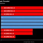
It shows a NVL 8+16+4 @ 4.8 GHz with a ST score of 5200 (from VideoCardz). While, CPU Mark ST score for 285K @ 5.7 GHz is 5087 (from official website).
This puts NVL ST performance uplift (vs 285K @ 5.7 GHz) at:
+ 2% @ 4.8 GHz
+21% @ 5.7 GHz
+28% @ 6.0 GHz
+32% @ 6.2 GHz
I'm still not sure of the final NVL boost clocks, but since it's on N2P, I'm guessing it'll be 6.0 GHz or higher.
And the really crazy part is, CPU Mark *DOES NOT* include APX performance uplift which is expected to be around 10% on average for APX-enabled applications (including benchmark apps). Note that PassMark 11.1 does not support Intel APX extensions as of now.
Assuming NVL hits 6.0 GHz, PassMark shows +28% ST uplift over 285K which is wild (without APX). With APX, it'll be +38%. 👀
So, either this is an elaborate hoax, or if true it's gonna be a wild ride for Intel enthusiasts & people are going to sell their kidneys to buy the high-end 52C bLLC SKU.
What do you think?
Source: VideoCardz
My post:
xitter.gq/Silicon_Fly/status/194…
VideoCardz:
videocardz.com/newz/intel-co…


Intel Nova Lake ST Performance Update:
(1) IPC uplift: Most of the leaks suggest greater than 5% to ~10% approx IPC uplift for Coyote Cove (vs Lion Cove). Arctic Wolf is expected to have even more (like >20% over Skymont), but not the current focus.
(2) Frequency Gains: NVL 8P+16E Tile will be on N2/N2P in 2026. So, we can expect more than 5% to 10% clock bump over 285K (from 6.0 GHz to 6.2+ GHz approx).
(3) AVX: In Geekbench 6 ST, NVL will get an additional boost in "subtests like Object Detection and Background Blur, where AVX‑512 contributes up to a 21% advantage". This gives around +5% ST overall uplift in GB6 simply due to AVX.
(4) Microsoft on APX: "In a future release, .NET plans to support Intel’s APX, which also adds new GPR registers that will surpass 64 in total. Thanks to the work we’ve done with the SVE registers, minimal changes will be required to extend support for Intel APX registers."
So, 5% to 15% performance uplift for APX-enabled applications. Existing x64 binaries require recompilation. All .NET apps will automatically benefit from APX-enabled .NET runtime. So, overall APX-enabled Windows application performance uplift should be around ~10% approx.
(5) Misc: If they're able to weed out ARL-related issues with memory controller, cache latency, NoC, ringbus frequency, etc, that might provide NVL additional performance. Around ~5% at best.
Summarizing Coyote Cove ST Performance Uplift (without bLLC) over 285K:
= IPC gains + Freq gains + AVX10.2 gains + APX gains + misc gains.
= (5% to 10%) + (5% to 10%) + 5% + 10% (if enabled) + 5%?
Conservative estimate (w/o APX) for Coyote Cove Geekbench 6 ST: +15% to +25% ST uplift over 285K.
ARL 285K Geekbench 6 ST = ~3,350
NVL 4xxK Geekbench 6 ST = ~4,000 (median)
(4,000 is the barest minimum. I actually expect somewhere around 4,100.)
Relaxed estimate for Coyote Cove with "APX-enabled" Geekbench 6 ST: +25% to +35% ST uplift over 285K.
ARL 285K Geekbench 6 ST = ~3,350
NVL 4xxK Geekbench 6 ST = ~4,350 (median)
(An APX-enabled GB6 test suite is not available at present.)
Take this with a grain of salt. But, Nova Lake (~4,100) may easily surpass Zen 6 and Apple M4 (3,870) in GB6 ST and may go neck to neck with Apple M5.
In short, Nova Lake *may* lead in ST (due to AVX, APX, µArch & >Fmax) and MT (due to 52 cores) and possibly Gaming as well (due to bLLC).
(Note: This is all about Geekbench 6 ST. These are estimates based on limited info and some leaks/speculation. Unlike ARL, NVL compensates Apple Silicon's GB6 ST SVE/SME advantage with APX, but they aren't identical. ARL has many small issues that addup and I'm assuming NVL fixes most of 'em. Also, % shouldn't be added, but let's keep it simple. Real world performance depends on workload and may vary. IPC/freq/AVX/APX info/leaks are already public.)
Keep reading... (1/3)

My last year (conservative) estimates:
xitter.gq/silicon_fly/status/194…
Intel X86S - Coming Back With A Vengeance!
Based on recent reports, Unified Core is now being developed by two different teams. First by Intel in Austin, Texas. The new one is RosaicLabs, Santa Clara.
So, what is Rosaic developing? All evidence points to a high-performance X86S-variant of Unified Core aimed at servers & AI (but I don't think it stop there).
Intel recently handed them access to E-core/Unified Core RTL. RTL stands for register-transfer level (hardware description of core logic).
X86S is a pure 64-bit only design. Dropping real mode, 16-bit protected mode, 32-bit protected mode including 32-bit ring 0. But instead, it still has 32-bit compatibility mode of x64 long mode.
This is not a hideous software translation layer like in Windows-on-ARM (WoA) x86 -> ARM. Same like Windows x64, X86S also directly executes 32-bit applications but with one minor caveat. Lack of 16-bit addressing.
Meaning, some rare legacy applications that use old 16-bit address-size overrides may not work. I'm talking about some 2 to 3 decade old legacy software with hand-coded assembly optimizations or legacy runtime libraries. Very rare these days.
RosaicLabs is currently working on the new X86S core and they're in collaboration with Intel. So, we can expect to hear from them probably by 2028 or 2029 at best. Earliest is, possible tapeout with Intel Uncore by 2028 at best imho.
Also, I've seen some dimwits assume X86S needs software emulation or translation layer or a VM to run 32-bit apps. That's completely wrong. They run 32-bit apps directly and exactly like your Windows 11 x64 but with slightly reduced backward compatibility for legacy applications that still use archaic 16-bit addressing. And those are mostly extinct already imho. So, not issues.
My estimate is X86S will have more than 99% compatibility with 32-bit apps. I think only 32-bit apps with hand optimized 16-bit assembly will have issues. And they don't matter anymore. The transition from x64 to X86S will be far smoother than the transition from Windows 32-bit to 64-bit.
X86S reduces x86 decoder complexity and improves efficiency. If x64 needs to catch up with the performance of ARM decoders and/or the likes of Apple Silicon, this is the most important step in the right direction. And it looks like Intel Austin team is risk-averse. And that's not good for Unified Core.
X86S is the right thing to do. And let's hope it happens. This is the way!
Share your thoughts. Follow/Repost if you like. 👍
Image Credit: VideoCardz

Pushkar Ranade - Intel CTO (on Intel Foundry vs TSMC)
"If you meant catching up in terms of technology, I think we're already there."
... The difference is within a few percentage points.
Chris Auth - Intel VP/GM of Manufacturing Development:
"14A will have High Quality PDK from the start."
Source: Dwarkesh Patel

TSMC: “We have no intention of leaving any food on the table for others.”
Meanwhile…
KeyBanc: “Intel Foundry wins with Apple are expected to be on 14A…”
😂😂😂
Thank god! Based on some reports, I was really worried that some high-end Nova Lake desktop tiles might end up on 18A-P. But that’s not the case.
All high end desktop tiles are on N2P. And that’s the way it should be for higher clocks and better thermals.
18A-P is best suited for laptop, mobile, server & ai parts. Not for high power, high frequency, high thermal desktop parts.


I’ll say it again:
Intel sharing 14A tech (and beyond) with Terafab is never good for Intel. When the news first came out, I was very worried. Now I’m happy it didn’t go through.
Simply put, Elon is one of the best there is when it comes to making deals. He’s that good. And once Terafab is fully operational and it doesn’t need Intel anymore, Intel will naturally get the royal shaft. Elon is that ruthless.
You don’t become a Trillionaire by throwing away money!
Thank god Intel didn’t go for the deal. 14A & beyond solely belongs to Intel and that’s the way it should be!
Share your thoughts…
Image credit: TechPowerUp


Gotta give it to my $INTC fam, yall really held it down after the Great Elon Betrayal of 2026. Market really said Elon/Terrafab don’t matter (yet).
LETS GO 🔥
Gr8 news! Intel Nova Lake with big fucking cache (BFC) is launching earlier that expected!
a.k.a bLLC

Riddle me this: 18A vs N3E
If we make the exact same die on Intel 18A and TSMC N3E, why on earth is the N3E die bigger by 20% ?
Yes. 20% bigger!!!
Like I said, 18A is a “2nm”’class node and not to be compared with any 3nm class process nodes.
More info:
SemiAnalysis on Intel 18A Density: A real banger!?
"Our measurements put Panther Lake’s 18A compute logic and TSMC N3E GPU logic at similar logic density. However, 18A does not lead TSMC N3P, N2 or Samsung SF2 in peak density."
First, Panther Lake CPU tile uses Intel 18A HP library. Whereas, Panther Lake iGPU uses the 2-2 HD library. Their statement comparing 18A & N3E is incorrect cos one is HP & the other is HD.
Second, they don't use Cell Utilization when comparing FSPDN/BSPDN nodes. Again, that's incorrect.
Lunar Lake CPU tile is 105 mm2 (without iGPU). Whereas, PTL-U 338H (4+0+4) CPU tile is only 91 mm2 (without iGPU). This is in spite of PTL-U 338H having extra 4MB L2 + 6 MB L3 cache. This size difference between the LNL & PTL CPU Tile is around 15%. If we remove this extra 10MB of cache from PTL-U and compare apples to apples, the difference is around 20%.
How is 18A able to pack more in significantly less area?
This is because of 18A higher "Cell Utilization". This puts 18A clearly ahead of *all* 3nm class nodes. 18A is close to N2 & 18A-P is closer to N2P.
The key purpose of BSPDN is to move the power rails, metals, grid, bumps to the backside, freeing up area in the front side. This freed up area in the frontside can accommodate more logic/sram. In a theoretical 100 mm2 pure FSPDN logic die (like TSMC N2P), only up to 75 mm2 can be used for pure logic. Whereas, in a theoretical 100 mm2 pure BSPDN logic die (like Intel 18A-P), over 90 mm2 can be used for pure logic according to Intel. This gives BSPDN nodes like 18A a solid edge in overall logic density. (Note: All density comparisons are theoretical peaks and not to be taken literally.)
So, w.r.t to my previous post, comparing densities of a FSPDN nodes like N2/N3 with a BSPDN nodes like 18A/18A-P without using Cell Utilization is a big mistake. Guaranteed to give wrong results.
Image Source: Semi Analysis
Link: newsletter.semianalysis.com/…
(For more details, see my previous post on this.)
Share your thoughts. Follow/Repost if you like. 👍
If you're wondering why Intel Nova Lake high-end high-frequency desktop CPUs are on TSMC N2P and not on 18A-P, the reason is simple:
FSPDN nodes (like N2P) have a solid advantage when to comes to high frequency designs like Zen 6 & Nova Lake. The heat can easily dissipate directly thru the TIM/IHS. Whereas, BSPDN nodes (like 18A) have some hotspot issues cos the heat has to dissipate thru additional metal layer and then thru the TIM/IHS. This additional layer reduces Fmax by a bit. But by how much exactly is still unknown, cos we never had a high frequency desktop design on 18A coupled with a large heat sink. My guess is, 18A Fmax penalty is around ~10% compared to N2 variants.
That's the reason Nova Lake high-end high-frequency SKUs are on N2P.
If NVL high-end desktop CPUs end up on 18A-P and has lower turbo frequency than Zen 6 top-end SKUs, I'd say, it's one of the worst decision Intel has ever made. I'm sincerely hoping NVL top-end 18A-P rumors are false.
Intel 18A vs TSMC N2P: 18A Kicks Ass!
We now have standard cell library metrics of N2P and 18A directly from Synopsys. Below is the chart that shows the logic densities and cell utilization of both N2P & 18A. Synopsys metrics attached below for reference.
In HD, density difference between N2P & 18A is only around 6.8%.
In HP, they're the same!
In SRAM, they're the same! (38.1Mb/mm2)
18A-P is a performance enhanced version of 18A, does not improve density. Both 18A & 18A-P are design rule compatible. Similarly, N2P is a performance enhanced version of original N2, does not improve density. Both N2 & N2P are design rule compatible.
When comparing logic densities of FSPDN & BSPDN process nodes, ignoring cell utilization is literally wrong, cos it gives completely wrong results. Simple reason is, FSPDN nodes (like TSMC N2P) have low cell utilization (lower than 75%) compared to BSPDN nodes (like Intel 18A) which have very high cell utilization (greater than 90%). If you're not using cell utilization when comparing densities, use effective densities instead.
FSPDN nodes (like N2P) have a solid advantage when it comes to high frequency designs like Zen 6 & Nova Lake. The heat can easily dissipate directly thru the TIM/IHS. Whereas, BSPDN nodes (like 18A) have some hotspot issues cos the heat has to dissipate thru additional metal layer and then thru the TIM/IHS. This additional layer reduces Fmax by a bit. But by how much exactly is still unknown, cos we never had a high frequency desktop design on 18A coupled with a large heat sink. My guess is, 18A Fmax penalty is probably around ~10% compared to N2 variants.
In essence, 18A is Intel's first true "2nm class" node.
Share your thoughts. Follow/Repost if you like. 👍


